CEG 2136 Lecture Notes - Lecture 4: Display Device, Instruction Register, Opcode

11 May 2018
School
Department
Course
Professor

LAB 4 BASIC COMPUTER ORGANIZATION
1. Objectives
In this laboratory, students will analyse the structure of a basic computer, will devise and design
its control unit, and will use opcodes to write simple programs in machine code. The design must
function in simulation, and also on the DE2-115 Altera development board.
2. Equipment and Supplies:
* Quartus II (student edition or web edition)
* Altera DE2-115 board with
- USB-blaster cable
- Power supply 12 VDC, 2A
3. References
You are provided with all the .bdf files, except one that describes the combinational circuits
which generates the output and transition functions of the Control Unit and which you are
expected to conceive and develop. Their logic diagrams are annexed to this document.
Chapters 5 and 6 of the textbook: Computer Systems Structures, Morris Mano, 3rd edition,
1993, ISBN 0-13-175563-3.
The course notes
The user guide of the Altera DE2-115 development kit is provided in the Laboratories >
Documentation section of your CEG2136 Blackboard
4. The Structure of the Basic Computer
4.1 General View
This laboratory implements a computer having a structure that is very close to the one presented in
figure 5.4 on page 130 of your textbook. However, there are two major differences:
1. The designed computer’s memory (storing both programs and data) has a capacity of 256 words
of 8 bits (256 x 8). In the textbook, the BASIC computer has a memory with words of 16 bits,
each word being capable of storing one memory-reference instruction (which consists there of a
4-bit opcode and a 12-bit memory address). In this lab, a memory-reference instruction is 2 byte
long as well, but the msb byte carries the opcode, while the lsb byte contains the operand address
(8 bits are enough to address a memory space of 28 = 256 memory locations); as such, a 2-byte
memory-reference instruction is stored in 2 consecutive memory locations (two 1-byte words).
As a consequence, two successive READ cycles are needed to fetch an instruction: first to get the
opcode, and the second to get the address of the data that the opcode will use.
2. The second major difference consists in the additional circuits which will allow a user to visualize
the contents of the memory independently of having a program running or not on the DE2-115
board.
User can preset the DIP switches on the board with the memory address to be visualized. Before
the fetch phase of each instruction, the BASIC computer reads the contents of the memory
location pointed at by the DIP switches on the board, and shows it in hexadecimal format on the 7
segment display of the board.
CEG 2136 Lab 4
EECS Lab 4 Page 2 of 22
University of Ottawa CEG2136: Computer Architecture I
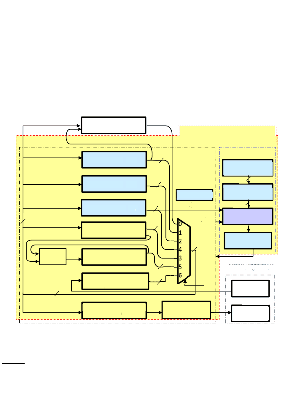
The block diagram of your computer is presented in Figure 1. The .bdf files of all the component
blocks, except the Instruction Decoder (lab_controller of CU), will be provided. The Control Unit
functions in accord with a time sequence which is generated by the sequence counter (SC) that plays
the role of FSM state register. The SC initial state is 0; it restarts counting from 0 at the beginning of
each instruction of a program and it is reset to 0 once that instruction is finished. A decoder converts
the 4-bit output of the SC into time-signals, distinct for each possible output (for example, when the
SC output is 0010, then the T
2
output of the decoder will go high, if not, it will remain low for any
other combination); this combination of the SC and its decoder implement a One-hot encoded state
register. The control commands for the Datapath are synthesized by the Instruction Decoder as (FSM
output) functions in terms of the contents of the IR, DR and other signals from the Datapath; a set of
gates (AND, OR, and NOT) forms the Instruction Decoder. As some CU outputs are of Mealy type, a
bank of buffer registers (Control Register) is used to insure a duration of one clock period for the
control commands that are generated by the CU, and to synchronize them with the system clock.
Figure 1: Computer block diagram
The following sequence of steps is repeated for each instruction cycle, as long as Stop Register = 0:
Display
1. The address of the memory location to being displayed (specified by the DIP switches) is
loaded from register OUTA to register AR.
2. The content of memory location at this address is loaded into OUTD whose output is connected
to the 7-segment display. Steps 1 and 2 are always executed, even if the system is in halt.
256x 8 Memory
Address registe
r
(A
R
)
Program counte
r
(PC)
Data registe
r
(D
R
)
Instruction registe
r
(I
R
)
INPUT Address REGISTE
R
(OUTA)
ALU
DIP switches
(addr. to display)
Sto
p
re
g
iste
r
Sequence counter
(SC) State Register
Instruction Decoder
(lab_controller)
Control Register
(Register bank)
State Decoder (T)
Bus
select
I
R
[7..0]
DR[7..0]
Control commands to
counters , registers ,
b
us
multiplexer and ALU
Data[7..0]
OUTPUT Data REGISTER
(OUTD)7-segment
displays
7-segment display
controllers
Control Unit Datapath
Accumulator
(
AC
)
I/O
CPU
Data[7..0]
Data[7..0]
Address [7..0]
4
16
8
8
8
8
8
8
8
8
8

CEG 2136 Lab 4
EECS Lab 4 Page 3 of 22
University of Ottawa CEG2136: Computer Architecture I
Fetch
3. The content of the Program Counter PC (containing at this point the address of the current
instruction) is loaded into AR (address register). PC determines the address of the memory
location from where the instruction is fetched (read) into the IR of the CPU. Since PC is reset to
0 whenever the UP2 board is programmed, your program’s first instruction has to be stored in
the first memory location (address 00).
4. PC is incremented to be prepared for getting the next instruction byte.
5. The first byte of the instruction (opcode) is fetched from memory and is stored in IR
(instruction register).
6. The IR content (instruction opcode) is decoded by the Instruction Decoder (in Control Unit).
7. If the instruction refers to a register, then skip to step 10.
8. If the instruction refers to memory, the PC content is transferred to AR, to get the second byte
of the instruction. This second byte of the instruction may contain
the address of the operand - if direct addressing mode; the instruction’s second byte (the
operand address) is read and directly loaded into AR;
the pointer to the operand address (i.e., address of the operand address) if indirect addressing;
This pointer is read from the memory location pointed by instruction’s 2nd byte and is loaded
to AR; then a newer read is performed to get the operand address and move it to AR.
The FETCH cycles conclude with AR carrying the operand address.
Execution
9. The data (operand) is read from the memory, and the PC is incremented to pointing to the next
instruction and being prepared for the next FETCH.
10. The EXECUTION cycles of the instruction are implemented, which requires typically several
more steps.
11. In the last cycle of the execution the SC is reset to 0, and the procedure begins again at step 1.
NOTE:
Setting Stop Register = 1=> blocks incrementing PC and stops running further instructions.
These steps will be discussed in detail below.
You will use a new type of file for memory initialization (.mif), to specify the contents of
memory; just go to “File” and open a “New” file which will display the list of file formats
from where you should select “Memory Initialisation File.” For this lab, the file .mif has to be
named memorycontents8.mif. To use hex numbers, you have to right-click on the Addr region
and then choose Hexadecimal for both Address and Memory (content) Radix. Save Every
time you change the contents of this file, you have to save and recompile your project.
Every time you want to run the program that you loaded in the memory, you have to
reprogram your device.
4.3 Syntax of the computer instructions
The instructions that can be executed by the computer are shown in Table 1. The second most
significant bit (IR6) specifies if the instruction is a memory-reference instruction (IR6=0) or a
register-reference instruction (IR6=1). The msb (I = IR7) specifies the instruction addressing mode
(direct or indirect), while the other bits form the opcode. For memory-reference instructions with
direct addressing mode another memory access is needed to read the operand, while two more
memory read cycles are needed to get the operand in case of indirect addressing. In conclusion,
register-reference instructions are encoded with one byte: {opcode},
memory-reference instructions employ a two byte format as follows:
o memory-reference instructions with direct addressing: {opcode, operand address}
o memory-reference instructions in indirect addressing: {opcode, address of the operand address}.
Document Summary
In this laboratory, students will analyse the structure of a basic computer, will devise and design its control unit, and will use opcodes to write simple programs in machine code. The design must function in simulation, and also on the de2-115 altera development board: equipment and supplies: * quartus ii (student edition or web edition) Power supply 12 vdc, 2a: references. You are provided with all the . bdf files, except one that describes the combinational circuits which generates the output and transition functions of the control unit and which you are expected to conceive and develop. Their logic diagrams are annexed to this document. Chapters 5 and 6 of the textbook: computer systems structures, morris mano, 3rd edition, The user guide of the altera de2-115 development kit is provided in the laboratories > Documentation section of your ceg2136 blackboard: the structure of the basic computer.