CEG 2136 Lecture Notes - Lecture 2: Computer Architecture, Sequential Circuits, Ribbon Cable

11 May 2018
School
Department
Course
Professor

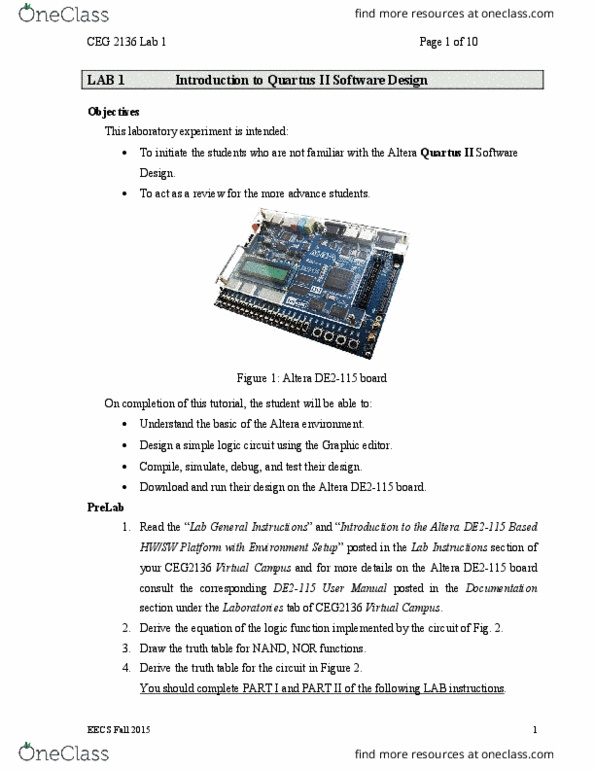
LAB 2 Design and Simulation of Sequential Logic Circuits
- Synchronous Counters -
1. Purpose:
This lab will enable students gain practice in the conversion of functional requirements into
logic circuits and their implementation using on the Altera DE2-115 board.
The purpose of this lab is to introduce students to the design of sequential circuits based on
Altera’s Quartus development environment and their implementation and testing with an
FPGA.
Enter the design of synchronous counters using Quartus II graphics editor
Assign the input-output pins and prepare the design for downloading and testing on
the Altera DE2-115 board
Test the counter:
- Display the counter outputs as binary values on LEDs
- Using an oscilloscope, trace and record the waveforms at various flip-flops.
2. Requirements of the Lab:
The following results need to be submitted in your report.
* The log of what you did
* The screen shots of all schematics and all waveform diagrams
* Compilation, simulation and downloading messages (if any)
* Your test results
3. Equipment and Supplies:
* Quartus II (web edition)
* Altera DE2-115 board with
- USB-Blaster cable
- Power supply 12V/2A
*Probe
*Coaxial cable
*Wires
*Ribbon cable
4. References:
i. Chapter1 and 2 of the Text book: Computer Systems Architecture, Morris Mano, 3rd Ed
ii. DE2-115 User Manual posted in the Documentation section under the Laboratories tab
of CEG2136 Virtual Campus.
5. PreLab
For each of the following counters (a. and b.):
Draw the state diagram and derive the excitation table for all the flip-flops
involved in the counter (the excitation table for counter a. is already given below),
Derive and simplify the Boolean expression of every flip-flop input using
Karnaugh maps.

CEG 2136 Lab 2 Page of 10
EECS Fall 2015
2
2
a. 3 bit synchronous modulo 6 counter
Block diagram in Fig. 1.(a), has to observe the following counting sequence: 000 --> 010
--> 110 --> 011 --> 101 --> 100 --> 000. This counter is to be implemented with JK flip
flops which have active-low asynchronous Reset inputs (CLRN); the flip-flops’ clock
inputs (CLK) are connected all together to CCLK (counter clock).
Figure 1: (a) Block diagram and
(b) State Diagram of a Modulo 6 counter
b. 4-bit synchronous BCD counter
Present
State Next
State Synchronous
Inputs
msb lsb
Q2Q1Q0 msb lsb
Q2Q1Q0 msb
J2K2
J1K1
lsb
J0K0
000 010 0 x 1 x 0 x
001 xxx x x x x x x
010 110 1 x x 0 0 x
011 101 1 x x 1 x 0
100 000 x 1 0 x 0 x
101 100 x 0 0 x x 1
110 011 x 1 x 0 1 x
111 xxx x x x x x x
Table 1: The Excitation Table for the JK
flip-flops Modulo 6 counter
0000 --> 0001 --> 0010 --> 0011 --> 0100 --> 0101
--> 0110 --> 0111 --> 1000 --> 1001 --> 0000 --> …
PART I (Design and simulation)
To capture your design in the Altera’s development environment you can use Quartus’
“New Project Wizard” or you can proceed manually with the following design flow.
For each circuit designed above (3 bit modulo 6 and 4-bit BCD synchronous counters):
1. Draw the circuit diagrams using the graphics editor of Quartus in a schematic
file and save the corresponding .bdf file. Use the counter’s signal names
suggested in the block diagram (Figure 1. a) when editing the names of the
pins of your circuit. In the Project Navigator pane select the Files tab; right-
click on your schematic file (.bdf) and select Set as Top Level Entity
Also save the schematics as a jpeg file or print it for inclusion in your report.
2. To assign EP4CE115F29C7 to your project go to Assignments in the main
menu, select Device and in the window Settings chose Cyclone IV E for the
Device Family and then from the list of Available Devices choose
EP4CE115F29C7.
000
0
1
0
110
011
101
100
Q2 Q1 Q0
CCLK
Reset

CEG 2136 Lab 2 Page of 10
EECS Fall 2015
3
3
In the main menu select Processing Start compilation or click on the toolbar
icon ► or press Ctrl+L.
3. To visualize the input and output signals of your counter (clock, reset, flip-
flops’ outputs) you have to create a University VWF file where you will catch
the time diagram of these signals.
4. To define the set of pins of your test circuit, while in the .vwf tab, do select in
the main menu Edit >> Insert >> Insert Node or Bus… and click on Node
Finder.
5. In the option Filter of the popped-up Node Finder window choose ‘Pins:
All’, then click on the button List and move all found nodes (from the left list)
to the right pane by clicking , then press OK to return to your .vwf files.
6. To set time characteristics of the simulation clock click on the clock signal
(CCLK) to select it, then do Edit >> Value>> Clock and in the Clock window
put a Period of 20 ns (a close approximation of the DE2-115 board clock)…
and click OK. Make sure you assign logic 1 to Reset by Forcing High (1), to
allow your counter operates under the CCLK control. At this point you can
run a functional simulation. The binary representation of the counter’s states
can be displayed by grouping Q2 – Q0 in a bus.
7. To choose a grid of 20 ns do: Edit >> Grid Size, then put 20 ns for Period.
Run your simulation (Processing Start simulation or click on the toolbar
icon ) and inspect the time diagram of your Simulation Report –
Simulation Waveforms window and verify if your synchronous counter
follows the given counting sequence; if it doesn’t, verify your equations
and/or debug your circuit.
NOTE: Make sure that under the simulator is the Quartus II simulator. Under
Simulation menu, go to Options and select Quartus II Simulator as the
simulator.
Show the simulation to your instructor and capture it in a graphic format for
your lab report (copy to clipboard all the waveforms and paste them into a
.doc file); to get a better visualization of your waveforms, you may want to
change the time base in your .vwf file by choosing in Edit/End Time a Time
Document Summary
This lab will enable students gain practice in the conversion of functional requirements into logic circuits and their implementation using on the altera de2-115 board. The purpose of this lab is to introduce students to the design of sequential circuits based on. Altera"s quartus development environment and their implementation and testing with an. Enter the design of synchronous counters using quartus ii graphics editor. Assign the input-output pins and prepare the design for downloading and testing on the altera de2-115 board. Display the counter outputs as binary values on leds. Using an oscilloscope, trace and record the waveforms at various flip-flops: requirements of the lab: The following results need to be submitted in your report. * the screen shots of all schematics and all waveform diagrams. * compilation, simulation and downloading messages (if any) * your test results: equipment and supplies: